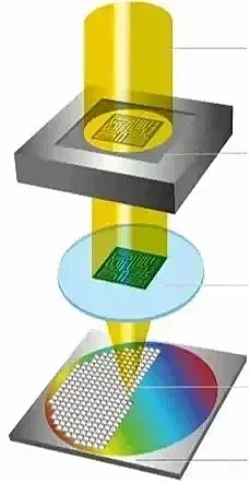
Lithography:
Thermal Control ±0.01°C to ±0.001 °C
Lithography includes several important stages where absolute temperature and temperature consistency are essential.
Mask Writing (E-Beam & Multi-Beam Systems)
Mask substrates (quartz, fused silica) have very low but nonzero coefficients of thermal expansion (CTE). A 1 mK fluctuation can shift pattern placement by nanometers across a 150 mm mask, unacceptable for sub-5 nm logic nodes.
Thermal Drift in MBMW.
Wafer Stage in EUV & Advanced ArF Scanners
Overlay budgets at 5 nm and below are ~2–3 nm. A 300 mm silicon wafer expands ~2.6 nm per 0.001 °C change. Without millikelvin control, pattern placement fails. Also, projection optics (mirrors in EUV) are highly sensitive to thermal drift.
Post-Exposure Bake (PEB) in Chemically Amplified Resists
Chemical amplification reactions double in rate with ~10 °C shift (Arrhenius). Even 0.01 °C variation changes diffusion length of photoacid, shifting line-edge roughness and CDs by 1–2 nm.
Metrology (Overlay & Critical Dimension Measurement)
Overlay metrology tolerances at 3 nm node are <2 nm. Thermal drift in the wafer stage or measurement optics introduces errors >spec if control isn’t millikelvin-level.
Projection Optics & Reticle Heating (EUV/DUV)
Projection optics are massive glass/mirror assemblies with extremely low but finite thermal expansion. A few millikelvin drift causes focus shifts and aberrations. Reticles under EUV exposure also heat, requiring active cooling at mK precision.
Metric ±0.5 °C ±0.1 °C ±0.01 °C
Overlay Drift ~100 nm ~60 nm ~30 nm—improved registration.
Photonic Coupling Loss ~1.0 dB ~0.5 dB ~0.2 dB—tighter alignment
of waveguides or lenses.
Resonator Drift ~10 pm/hr ~5 pm/hr ~1 pm/hr–better laser/modulator. (Wavelength) locking.
Stage Drift ~40 nm/hr ~20 nm/hr. ~5 nm/hr,more stable,
metrology, probing, and bonding.